Today, we will take a closer look at understanding the chip packaging process and testing, often called the “packaging and testing” stage. This stage, also known in the semiconductor industry as the backend process, is usually handled by OSAT (Outsourced Semiconductor Assembly and Test) companies.
Understanding Chip Packaging Process: Purpose of Encapsulation
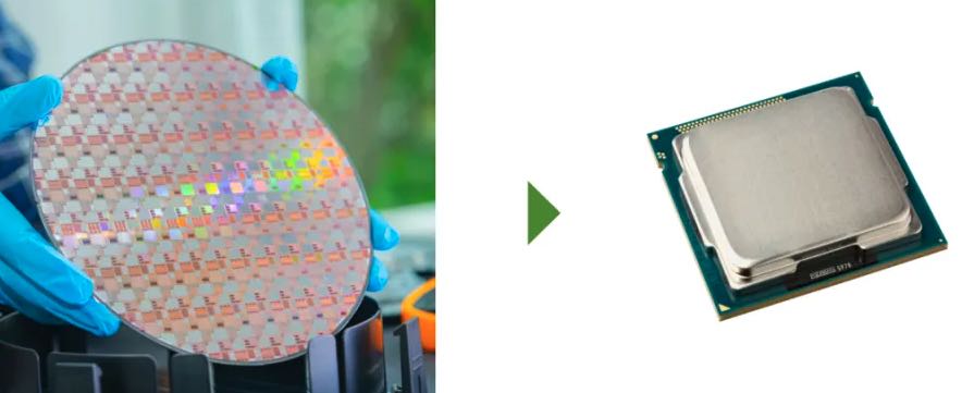
When we talk about “packaging,” we mean the process of transforming bare chips (dies) from a wafer into the final finished products we see in devices. Chip encapsulation serves two main purposes.
First, it protects the fragile silicon die from physical damage and prevents air impurities from corroding the delicate circuit structures.
Second, it ensures that the chip can adapt to various usage environments. Since chips are used in many different applications, each with specific requirements for size and performance, proper packaging helps the chip function reliably under different conditions.
Stages of Packaging Development
Chip packaging technology has evolved alongside integrated circuits for more than 70 years. Broadly, it has gone through five major stages of development.
Traditional Chip Packaging
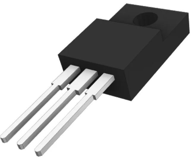
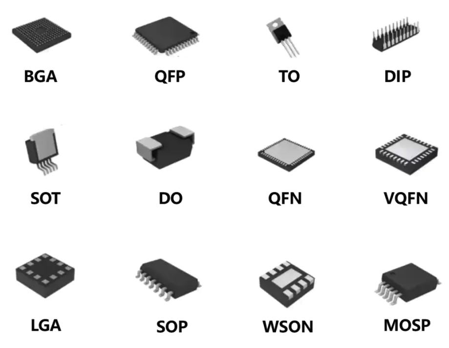
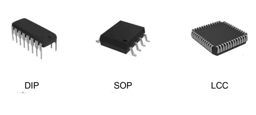
The earliest transistors used TO (Transistor Outline) packages. Later, DIP (Dual In-line Package) became popular. PHILIPS later developed SOP (Small Outline Package), which led to variants like SOJ (J-pin Small Outline Package), TSOP (Thin Small Outline Package), VSOP (Very Small Outline Package), SSOP (Shrink SOP), TSSOP (Thin Shrink SOP), SOT (Small Outline Transistor), and SOIC (Small Outline Integrated Circuit).
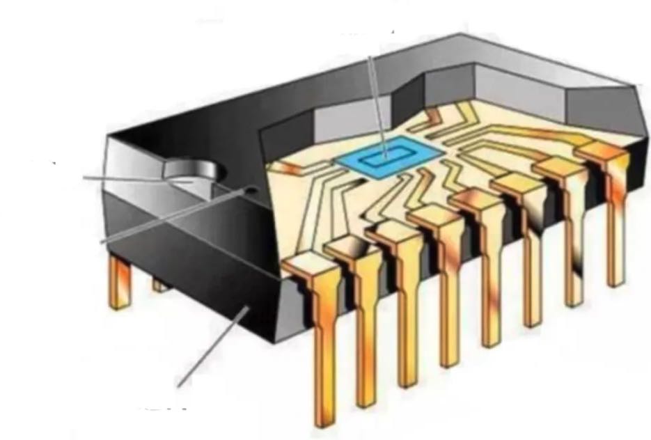
Between the 1960s and 1990s, these through-hole (THP) and surface-mount (SMP) packages dominated and are now referred to as traditional packaging methods. They rely mainly on metal wires to connect the chip die to external circuits.
Many of these packages are still in use today, especially in older or low-cost chip models that do not require high performance or miniaturization.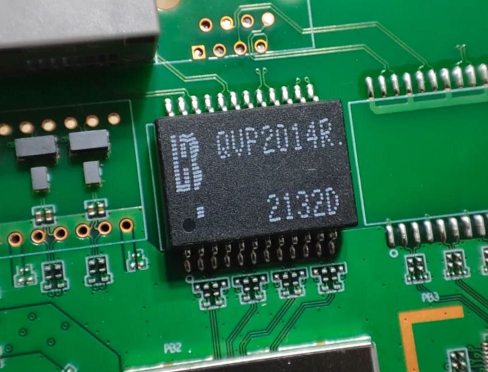
The Shift to BGA and Grid Arrays
 By the 1990s, as IT technology advanced rapidly, chips became more complex and required more pins. With devices shrinking in size, new packaging approaches were needed.
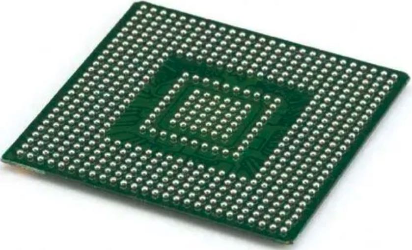
This led to the rise of BGA (Ball Grid Array) packaging, which soon became mainstream. BGA packages have pins located beneath the chip, making them compact and suitable for components needing numerous connections. Similar types include LGA (Land Grid Array) and PGA (Pin Grid Array)—all commonly seen in CPUs today.
Advanced Chip Packaging
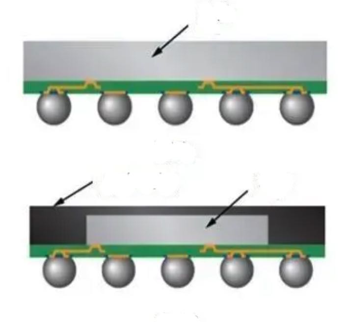
In the late 20th century, newer forms such as CSP (Chip-Scale Packaging), WLP (Wafer-Level Packaging), and Flip-Chip Packaging appeared, marking the shift from traditional to advanced packaging.
 CSP focuses on minimizing size; the package area is usually no more than 1.2 times that of the chip itself. WLP takes this further, with packaging performed directly on the wafer before dicing, unlike traditional methods, where the wafer is diced first.
Flip-chip packaging eliminates wire bonding entirely. Instead, the chip is flipped over and connected to the substrate through microscopic solder bumps. Originally invented by IBM in the 1960s, it became widely adopted in the 1990s.
Compared to wire-bonded packages, flip-chip designs offer more I/O channels, shorter electrical paths, improved performance, better heat dissipation, and smaller overall size.
It uses improved designs and modern processes to rebuild the chip structure at the packaging level. This allows for more pins, a smaller size, and higher system integration, which together boost performance and efficiency.
In the 21st century, the growth of mobile communication and the internet pushed chip packaging toward smaller, faster, cheaper, and more reliable designs. Advanced packaging has entered a rapid development phase.
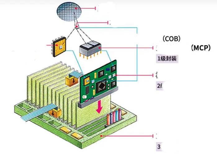
During this stage, chip structures evolved from flat two-dimensional layouts to three-dimensional stacking, where multiple dies are combined in one package. New technologies such as 2.5D and 3D packaging, through silicon vias (TSV), redistribution layers (RDL), fan-in and fan-out wafer-level packaging, and system-in-package (SiP) were introduced.

As chip manufacturing reaches the limits of Moore’s Law, these new packaging methods have become a key path for keeping progress alive.
Key Technologies of Advanced Packaging
2.5D and 3D Packaging
 Both 2.5D and 3D technologies involve stacking chips.
2.5D packaging allows two or more chips to be placed in one package, where signals can move sideways through a silicon interposer. This helps reduce size and improve performance.
3D packaging stacks chips vertically, using drilled holes and internal wiring to connect the layers directly. This design is harder to build but delivers higher speed and density.
These technologies are often used in memory and high-performance devices. For example, High Bandwidth Memory (HBM) uses both 2.5D and 3D stacking to connect memory and GPU chips for faster processing.
System-in-Package (SiP)
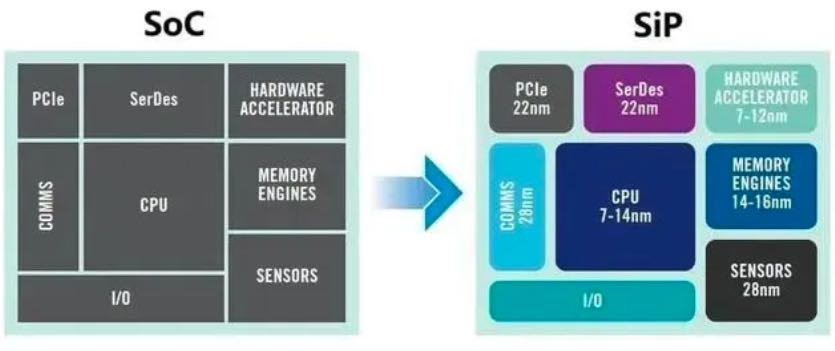 System-on-Chip (SoC) combines many functions in one chip, but it is complex and costly to design. SiP offers a flexible and lower-cost option. It packages multiple chips side by side or stacked into one unit.
SiP is the base for the popular “chiplet” design, which links several small dies together to create one powerful unit.
Through Silicon Via (TSV)
A TSV is a vertical channel etched into silicon and filled with metal to link the upper and lower layers of a chip. These short connections support smaller, faster, and more efficient 3D structures.
Redistribution Layer (RDL)
An RDL adds a thin metal layer to reroute input and output ports to new positions, improving how chips connect within a package. It enables flexible connections in both horizontal and vertical directions.
Fan-In and Fan-Out Wafer-Level Packaging
 In fan-in packaging, the chip is packaged directly on the wafer, keeping the same size as the chip. Fan-out packaging rearranges the diced chips before packaging, allowing wiring to extend beyond the chip area. This supports more pins and better performance.
Today, fan-out designs are the most widely used in mass production. These are the basics of how chip packaging evolved and the key technologies behind it.
Leave a Reply